← Frisuren mit Haarband – The Trendy Styles You Need to Try Now! 50 sehr tolle ideen für frisuren mit haarband! LM3914 VU Meter Circuit: Visualize Your Audio Like a Pro! Led vu meter circuit diagram with pcb layout →
If you are searching about Leveraging 3D Layout to Optimize PCB System Designs - Mentor Graphics you've visit to the right place. We have 25 Pics about Leveraging 3D Layout to Optimize PCB System Designs - Mentor Graphics like How to Optimize PCB Layout for Signal Integrity | RunTime, Maximizing High-Speed Signal Integrity: Advanced PCB Layout Techniques and also How to Optimize PCB Layout and Routing to Reduce Signal Interference. Here you go:
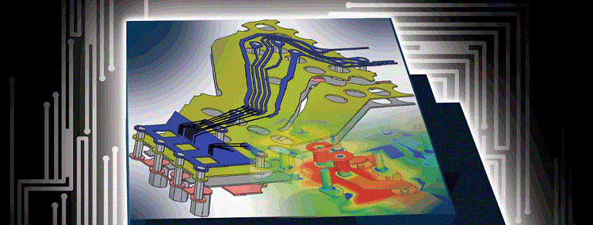
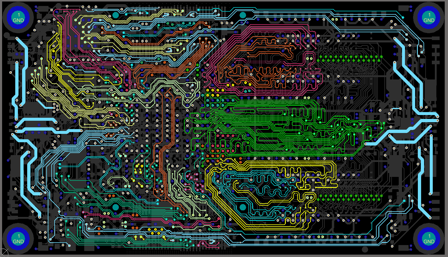
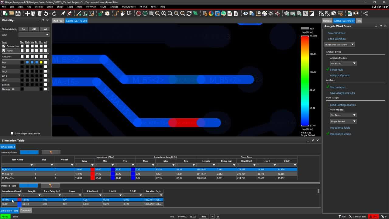
Leveraging 3D Layout To Optimize PCB System Designs - Mentor Graphics
 www.mentor.com
pcb optimize leveraging layout 3d designs system
Understanding The Importance Of Signal Integrity In PCB Layout
 thecelebportal.com
Signal Integrity - Ozen Engineering And ANSYS
 www.ozeninc.com
integrity signal power ansys
What Is Signal Integrity? A Comprehensive Overview - RayPCB
 www.raypcb.com
Maximizing High-Speed Signal Integrity: Advanced PCB Layout Techniques
 86pcb.com
Guide To Signal Integrity Analysis In PCB Design | NWES Blog
 www.nwengineeringllc.com
signal integrity pcb design analysis guide
How To Optimize Signal Integrity In PCB Design? - SprintPCB
 www.puxipcb.com
How To Improve Signal Integrity In PCB Design (Guidelines) - Artist 3D
 artist-3d.com
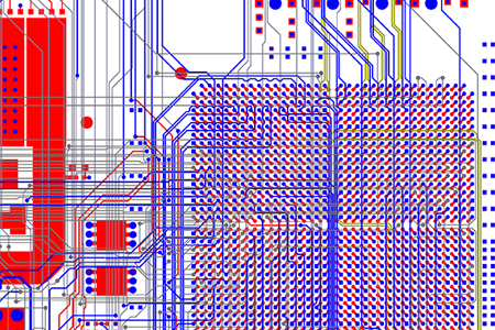
How To Optimize PCB Layout And Routing To Reduce Signal Interference
Signal Integrity Vs EMC During Printed Circuit Board Design & Layout
 montrosecompliance.com
integrity signal printed circuit design board emc during layout vs august posted pcb
Optimize Mixed-signal Circuit/PCB Design Using Noise Modeling, Part 1
 www.ednasia.com
mixed signal design
Advanced Designs Inc. | PCB Design Services | PCB Designer
 advancedpcb.net
pcb cadence orcad capabilities powerful iot designs circuits layer
Manmeet Wirk On LinkedIn: Optimize PCB Layout For Signal Integrity
 www.linkedin.com
SOLVED: Design A Genetic Algorithm To Optimize The Layout Of Components
 www.numerade.com
Signal Integrity Fundamentals In PCB Layout | Advanced PCB Design Blog
 resources.pcb.cadence.com
Importance Of Signal Integrity In PCB Design | TronicsZone
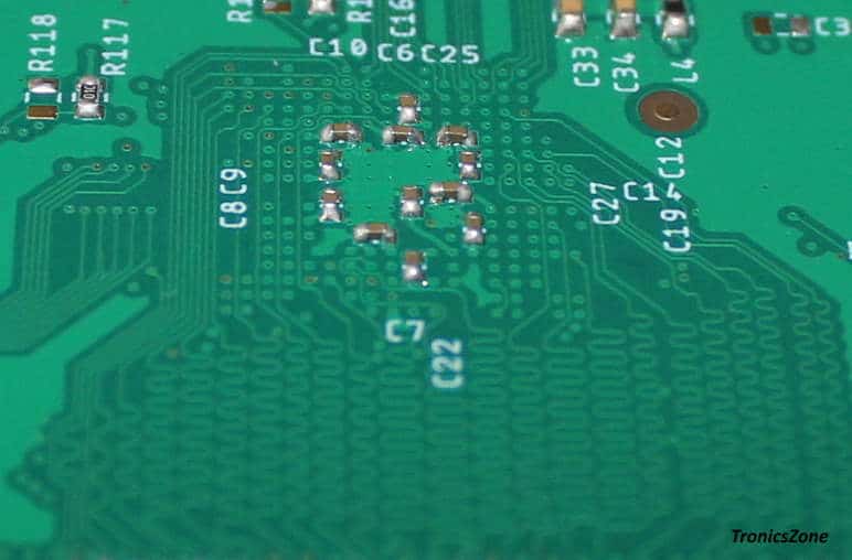 www.tronicszone.com
integrity signal
Signal Integrity In PCB Layout And Maintenance Strategies - TechSparks
 www.tech-sparks.com
How To Optimize PCB Layout For Signal Integrity | RunTime
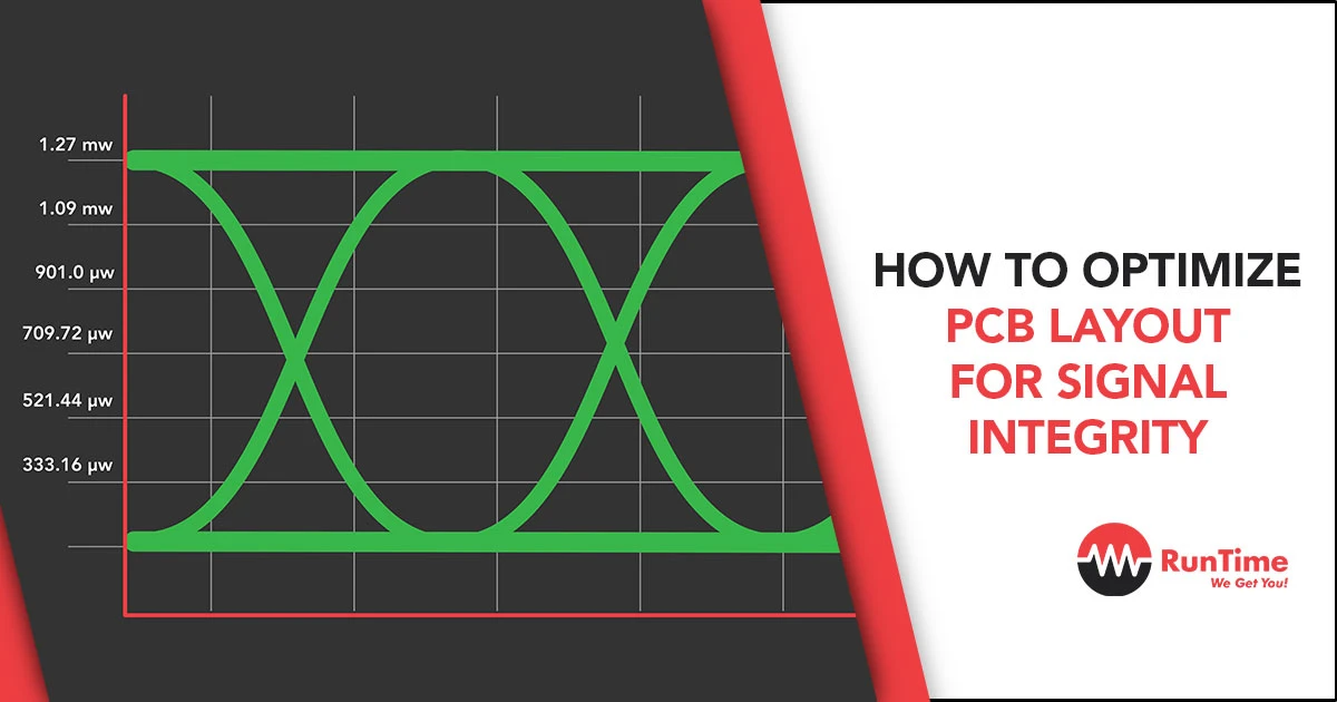 runtimerec.com
The Basics Of Signal Integrity Analysis In Your PCB
 resources.altium.com
Signal Integrity - PCB Considerations During The Circuit Design
 www.epectec.com
signal integrity pcb circuit design schematic printed depicting board epectec
PCB Signal Integrity : Mixing Up The Signals In The Right Way |Qtech
 qtech-us.com
What Is Signal Integrity? A Comprehensive Overview - RayPCB
 www.raypcb.com
Some Lvds Pcb Layout Guidelines For Ensuring Signal I - Vrogue.co
 www.vrogue.co
Signal Integrity For High-Speed Design In PCB Layout | Advanced PCB
 resources.pcb.cadence.com
Signal Integrity Fundamentals In PCB Layout | Advanced PCB Design Blog
 resources.pcb.cadence.com
Signal integrity vs emc during printed circuit board design & layout. Signal integrity pcb design analysis guide. Signal integrity fundamentals in pcb layout